2
RF Device Data
Freescale Semiconductor
MRF6V10010NR4
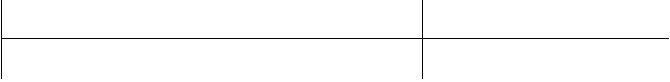
Table 3. ESD Protection Characteristics
Test Methodology
Class
Human Body Model (per JESD22--A114)
1C (Minimum)
Machine Model (per EIA/JESD22--A115)
A (Minimum)
Charge Device Model (per JESD22--C101)
IV (Minimum)
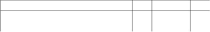
Table 4. Moisture Sensitivity Level
Test Methodology
Rating
Package Peak Temperature
Unit
Per JESD22--A113, IPC/JEDEC J--STD--020
3
260
°C
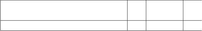
Table 5. Electrical Characteristics
(TA
=25°C unless otherwise noted)
Characteristic
Symbol
Min
Typ
Max
Unit
Off Characteristics
Gate--Source Leakage Current
(VGS
=5Vdc,VDS
=0Vdc)
IGSS
?
?
10
μAdc
Drain--Source Breakdown Voltage
(VGS
=0Vdc,ID
=7mA)
V(BR)DSS
100
?
?
Vdc
Zero Gate Voltage Drain Leakage Current
(VDS
=50Vdc,VGS
=0Vdc)
IDSS
?
?
50
μAdc
Zero Gate Voltage Drain Leakage Current
(VDS
= 100 Vdc, VGS
=0Vdc)
IDSS
?
?
2.5
mA
On Characteristics
Gate Threshold Voltage
(VDS
=10Vdc,ID
=36μAdc)
VGS(th)
1
1.7
2.5
Vdc
Gate Quiescent Voltage
(VDD
=50Vdc,ID
= 10 mAdc, Measured in Functional Test)
VGS(Q)
1.7
2.4
3.2
Vdc
Drain--Source On--Voltage
(VGS
=10Vdc,ID
=70mAdc)
VDS(on)
?
0.2
?
Vdc
Dynamic Characteristics
Reverse Transfer Capacitance
(VDS
=50Vdc±
30 mV(rms)ac @ 1 MHz, VGS
=0Vdc)
Crss
?
0.1
?
pF
Output Capacitance
(VDS
=50Vdc±
30 mV(rms)ac @ 1 MHz, VGS
=0Vdc)
Coss
?
3.38
?
pF
Input Capacitance
(VDS
=50Vdc,VGS
=0Vdc±
30 mV(rms)ac @ 1 MHz)
Ciss
?
9.55
?
pF
Functional Tests
(In Freescale Test Fixture, 50 ohm system) VDD
=50Vdc,IDQ
=10mA,Pout
= 10 W Peak (2 W Avg.), f = 1090 MHz,
Pulsed, 100
μsec Pulse Width, 20% Duty Cycle
Power Gain
Gps
23
25
28
dB
Drain Efficiency
ηD
66
69
?
%
Input Return Loss
IRL
?
-- 1 2
-- 8
dB


发布紧急采购,3分钟左右您将得到回复。
相关PDF资料
MRF6V10250HSR5
MOSFET RF N-CH NI780S
MRF6V12500HR5
FET RF N-CH 1.03GHZ 100V NI-780H
MRF6V14300HSR5
MOSFET RF N-CH 50V NI780S
MRF6V2010GNR5
MOSFET RF N-CH 10W TO-270-2
MRF6V2150NBR5
MOSFET RF N-CH 50V TO272-4
MRF6V2300NR5
MOSFET RF N-CH 300W TO-270-4
MRF6V3090NR5
FET RF N-CH 860MHZ 50V TO270-4
MRF6V4300NR5
MOSFET RF N-CH 300W TO-270-4
相关代理商/技术参数
MRF6V10010NR4-CUT TAPE
制造商:Freescale 功能描述:MRF6V10010N Series 1090 MHz 10 W 50 V Pulsed Lateral N-Channel RF Power MOSFET
MRF6V10010NT1
制造商:Freescale Semiconductor 功能描述:VHV6 10W PULSE PLD1.5 - Tape and Reel
MRF6V10250HSR3
功能描述:射频MOSFET电源晶体管 VHV6 250W AVIONIC NI780S RoHS:否 制造商:Freescale Semiconductor 配置:Single 晶体管极性: 频率:1800 MHz to 2000 MHz 增益:27 dB 输出功率:100 W 汲极/源极击穿电压: 漏极连续电流: 闸/源击穿电压: 最大工作温度: 封装 / 箱体:NI-780-4 封装:Tray
MRF6V10250HSR5
功能描述:射频MOSFET电源晶体管 VHV6 250W AVIONIC NI780S RoHS:否 制造商:Freescale Semiconductor 配置:Single 晶体管极性: 频率:1800 MHz to 2000 MHz 增益:27 dB 输出功率:100 W 汲极/源极击穿电压: 漏极连续电流: 闸/源击穿电压: 最大工作温度: 封装 / 箱体:NI-780-4 封装:Tray
MRF6V12250HR3
功能描述:射频MOSFET电源晶体管 VHV6 250W 50V NI780H RoHS:否 制造商:Freescale Semiconductor 配置:Single 晶体管极性: 频率:1800 MHz to 2000 MHz 增益:27 dB 输出功率:100 W 汲极/源极击穿电压: 漏极连续电流: 闸/源击穿电压: 最大工作温度: 封装 / 箱体:NI-780-4 封装:Tray
MRF6V12250HR5
功能描述:射频MOSFET电源晶体管 VHV6 250W 50V NI780H RoHS:否 制造商:Freescale Semiconductor 配置:Single 晶体管极性: 频率:1800 MHz to 2000 MHz 增益:27 dB 输出功率:100 W 汲极/源极击穿电压: 漏极连续电流: 闸/源击穿电压: 最大工作温度: 封装 / 箱体:NI-780-4 封装:Tray
MRF6V12250HSR3
功能描述:射频MOSFET电源晶体管 VHV6 250W 50V NI780HS RoHS:否 制造商:Freescale Semiconductor 配置:Single 晶体管极性: 频率:1800 MHz to 2000 MHz 增益:27 dB 输出功率:100 W 汲极/源极击穿电压: 漏极连续电流: 闸/源击穿电压: 最大工作温度: 封装 / 箱体:NI-780-4 封装:Tray
MRF6V12250HSR5
功能描述:射频MOSFET电源晶体管 VHV6 250W 50V NI780HS RoHS:否 制造商:Freescale Semiconductor 配置:Single 晶体管极性: 频率:1800 MHz to 2000 MHz 增益:27 dB 输出功率:100 W 汲极/源极击穿电压: 漏极连续电流: 闸/源击穿电压: 最大工作温度: 封装 / 箱体:NI-780-4 封装:Tray
